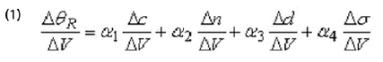
Voltametric technique in electrochemical (EC) detection is a very powerful analytical method that has been used for a wide range of applications. When combined with SPR technology, EC-SPR provides many insights into various electrochemical phenomena and processes taking place at solid-liquid interfaces, including charge-induced molecular adsorption/desorption and structural changes of adsorbates, electrodeposition, and anodic stripping.
In EC-SPR, the thin metal film not only serves to excite surface plasmons, but also acts as a working electrode for electrochemical detection.
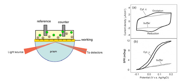
FIG. 1
By controlling the potential of the working electrode – a SPR metal sensor (shown left) with respect to a reference electrode using a potentiostat, electrochemical processes can be studied by monitoring both the current and the SPR signal at the electrode
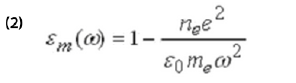
A change in the electrode potential (∆V) can shift the resonance angle (∆θR) via different effects. Typically these effects include changes in the molecular coverage (∆c), index of refraction (∆n) and average thickness of the adsorbed layer. An additional effect is the potential-induced change in the surface charge density (∆σ) of the electrode. These effects can be written as the formula shows. Where α1 , α2 , α3 and α4 are constants for a small potential change.
The first term in the above equation is due to potential-induced adsorption or desorption. The second term describes changes in the electronic states of the adsorbed layer, which can arise from the Stark effect, structural changes, or chemical reactions of the adsorbates. The third term is due to the change in the thickness of the molecular layer, from structural change and piezoelectric effect. The piezo-electric effect is usually a small constant. The last term is due to potential-induced changes in the dielectric constant of the metal film, εm, via the electron density, ne, according to the simple free electron model of metals,
where e and me are the charge and mass of electron, respectively.
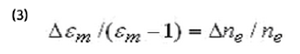
The change of εm due to ne is:
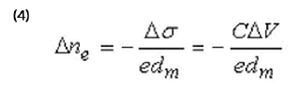
Where ∆ne is related to the potential-induced excess surface charge,
∆σ = C∆V (C interfacial capacitance), and given by:
Where dm is the thickness of the metal film.
EXAMPLE
For a 50 nm silver film, dm = 50 nm, ne = 5.85 x 10²² /cm2,em = -11.8 , and C = 20 m F/cm2, which leads to Dem ~ -0.002 per volt, corresponding to an angular shift of ~0.02° per volt. Since this contribution is proportional to the interfacial capacitance, it decreases when the metal film is covered with molecular adsorbates.
By Nguyen Ly | Biosensing Instrument | Published March 1, 2010